When drawing a schematic, crossing wires can make the schematic difficult to read and follow signals (see example, Figure 1). This tutorial shows several techniques for keeping your schematic tidy.
Figure 1: Example of difficult-to-follow schematic
How do I keep my schematic tidy?
Technique 1: Lay out parts to avoid crossing wires
You can edit the pin layout of a schematic symbol to avoid crossing wires (see Figure 2).
Figure 2: Schematic symbol edited to avoid crossing wires
Technique 2: Use Net Aliases
Net aliases let you make connections across the schematic without wires. Nets (wires) with the same name are electrically connected.
Figure 3: Place net alias tool
Figure 4: Schematic using net aliases
Technique 3: Use Multiple Pages
You can also create multi-page schematics and use off-page connectors (similar to net aliases) to make electrical net connections across pages.
Technique 4: Boxes and Labeling
An excellent way to help make your schematic more readable is to use the box tool and the text tool to section off and label different areas of the schematic. Also, make sure to complete your title block.
Figure 5: Example schematic with sections and labels
Based on a tutorial written by Robert Goby. Updated by Zachary Conley.
When drawing a circuit, you will often move and delete components as part of the process, meaning that the reference designators (e.g., R1, C1, U1) may be out of order or scattered throughout your design. This tutorial walks through how to reset the reference designators so they are sequential.
WARNING: Do not reset the reference designators after you have moved a design to PCB Editor, or it may break links between the schematic and PCB layout.
How do you reset the reference designators in Cadence Design Entry CIS?
1. Open your schematic in Design Entry CIS
2. In Design Entry CIS, select the root folder for your schematic and click the Annotate button in the toolbar (see Figure 1). The Annotate window will appear (see Figure 2).
Figure 1: Annotate tool
Figure 2: Annotate Window
3. In the Annotate window (see Figure 2), choose Action > Reset part references to "?". Click OK.
4. Click the Annotate button again, and this time choose Action > Incremental reference update. Click OK. Your reference designators are now renumbered!
Based on a tutorial written by Robert Goby and updated by Ryan Sparks
A via is an electrical interconnection that connects one layer of a PCB to another layer of a PCB. Vias are typically used when two wires need to cross on the same side of a PCB design, but cannot without continuing the trace on a different layer. It is best to minimize the use of vias for boards being manufactured in Peralta to maximize reliability, but sometimes they are necessary in order to complete a design. If you do need a via, the default via padstack in Cadence is too small for the LPKF ProtoMat S63 PCB Mill that we use to manufacture PCBs in PRLTA 109. There are two ways to address this issue:
Place all of your vias, and then replace them with the provided asuvia.pad padstack (provided in the Cadence installation instructions you followed earlier in the semester).
Change the size of the drill and pad on the Cadence default via.pad padstack.
1.0: Replacing your existing vias with the asuvia.pad padstack
1.1. In Windows, lay out the traces and vias on your board, minimizing the number of vias used.
1.2. Right-click on one of the vias and select Replace Padstack > All instances (see Figure 1 below)
Figure 1: Using "Replace Padstack" to change all instances of a via padstack
1.3. Select the asuvia.pad Padstack from the list of available padstacks (see Figure 2 below) and click OK. Note: This will only work if you have configured Cadence properly according to our provided instructions, and your Cadence\symbols folder contains asuvia.pad
Figure 2: Selecting the asuvia padstack
2.0: Changing the default via.pad padstack
As an alternative to using asuvia.pad, you can instead change the default via.pad padstack. You do not need to do both.
2.1. In Windows, open Padstack Editor
2.2. Choose File > Padstack Library Browser... and choose via.padfrom the list (see Figure 3). Click OK.
Figure 3: Choosing via.pad from the Library Padstack Browser
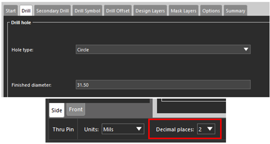
2.3. In the Drill/Slot hole section, set the Drill diameter to 31.5 and change your "Decimal places:" to 2 (see Figure 4).
Figure 4: Drill diameter set to 31.50
2.4. Click the Design Layers tab (see Figure 5) and change the settings for the BEGIN LAYER, DEFAULT INTERNAL, and END LAYER. Click the Mask Layerstab (see Figure 6) and change the settings for SOLDERMASK_TOP and SOLDERMASK_BOTTOM.
Figure 5: Design Layers tab with layers configured
Figure 6: Mask Layers tab with layers configured
2.5. Choose File > Save and overwrite the existing file. You have now successfully changed the default via size to be manufacturable and handle up to 5 amps of current!
Note: If you are working on the computers in Peralta Studios, you may not be able to change and save the default via because of file permissions. Instead, simply change the padstacks to use the asuvia.pad after you are done designing the board.
The following video shows the process described in this tutorial from start to finish in Cadence 16.6 (old version):
Based on a video and tutorial created by Robert Goby and updated by Qinchen Zha (2/2020) and Ryan Sparks (10/2020).
Text is important on PCB layouts to identify the designers, project, version, components, etc. Typically, text can be placed on a silkscreen layer that sits on top of the copper. However, our manufacturing process in PRLTA 109 only supports text that is milled on the TOP COPPER or BOTTOM COPPER layers.
Note: It is required that all PCB designs have your name, course, and team number so that the Peralta Engineering Studios staff can distinguish your board from others.
How do you create millable text in Cadence PCB Editor?
1. Open your design in PCB Editor
2. Choose Setup > Design Parameters... and click the Text tab. Click the ... button next to Setup text sizes (see Figure 1). The Text Setup window will open (see Figure 2).
Figure 1: Design Parameter Editor Text tab
Figure 2: Text Setup window
2. In the Text Setup window, change the Photo Width for Text Blk 4 to 10.00 (see Figure 2). The 4th text value is big enough to read but not overly large. Click OK and OK to return to your design.
3. Click the abc+ button in the toolbar (see Figure 3) and click on the Options tab on the right hand of the screen (see Figure 4).
Figure 3: Add Text button
Figure 4: Options tab configured for the 4th text block
4. Configure the options to make sure the Top or Bottom layer is selected, and that the Text block is set to 4 (or whichever one that you changed in step 2) (see Figure 4).
5. Click anywhere on the board and type the text that you wish to add (see example, Figure 5).
Note: This tutorial shows how to print a PCB design on paper. Please see the ASU PCB Fabrication Process for instructions on how to manufacture / "print" a PCB design in copper.
Why would you want to print a PCB design on paper?
Before sending a PCB to be manufactured, it is imperative to separate the layers and print it at 1:1 (100%) scale on paper to physically verify that your parts will fit through the holes and that pad spacing is correct.
2. In the Layer Display window, right-click on a layer and choose All Layers Off.
3. Pick a layer and click the light bulb icon next to the layer name to enable it.
4. Highlight the enabled layer in the workspace. Right-click on the enabled layer and choose Move from the contextual menu. Left-click anywhere in the workspace and then move the layer somewhere off to the side so that it won't overlap with the other layers. Left click again. Right click anywhere in the workspace to exit the "Move" mode.
5. Repeat steps 3 - 5 for the remaining layers in your design (see example, Figure 1)
Figure 1: Example of separated layers
6. Choose File > Print... and select Plot Scale : User Scale of 1.0. Click Next and PLOT! to print your design.
Designs created in an ECAD program may be electrically correct on the screen, but are ultimately constrained by the capabilities of your fabrication equipment. This tutorial walks through how to use the program DFM Now to verify that a design is able to be manufactured by the LPKF ProtoMat S63 in PRLTA 109.
This tutorial requires that you have already exported Gerber files of your design from Cadence.
The following video shows the process described in this tutorial from start to finish.
Download the Peralta Mill Specs.drf configuration file and save it to a known location. This file contains customized settings that will allow you to use DFM
Step 2: Run DFM Now on the Gerber Files
1. In Windows, launch DFM Now!
2. Choose Import > AutoLoad (Gerber/Drill)..., select the folder that contains the Gerber and drill files for your project, and click Next (see Figures 1 and 2).
Figure 1: AutoLoad import menu
Figure 2: Select Folder to Load window
3. In the File Description: window (see Figure 3), choose the correct layer type for each layer. Common layer types include:
Top Art = Top
Bottom Art = Bottom
Outline = Border (this is typically a graphic and may be the only one that you need to change)
Soldermask Top = Mask Top
Soldermask Bottom = Mask Bottom
Drill = Drill ThruHole
Figure 3: File Description window
4. Click Next and Finish.
5. Review your design and make sure all of the layers were loaded properly.
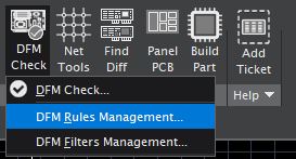
6. Choose DFM > DFM Rules Management... (see Figure 4). The DFM Check Settings window will appear (see Figure 5).
Figure 4: DFM Rules Management menu selection
Figure 5: Default DFM Check Settings window
7. In the DFM Rules Settings window under Rules File Management, click Open... and choose the Peralta Mill Spec.drf file that is saved to your hard drive. Under Rules File Management, click Save As... and save the rules so they are available next time you open the program. New DFM settings will appear in the Signal tab (see Figure 6). Click Finish.
8. Choose DFM > DFM Check.... The General Settings window will appear (see Figure 7). Make sure that the DFM Rule Set is set to Peralta Mill Specs.drf and click Next to begin the design for manufacturing process.
Figure 7: General Settings window
9. Depending on the complexity of your board, the DFM check will take several seconds to several minutes to run. If it uncovers any errors, you will need to find and correct them within PCB Editor, re-export your Gerber files, and re-run the DFM Check on the new Gerber files.
10. Once you have corrected all of the errors, you will receive a green checkmark. Success! (see Figure 8)
Figure 8: Example errors and success
11. Bring your computer to a TA or professor during office hours and show them the results of your DFM check to receive approval for submitting your PCB design to Peralta for milling.
Based on a video and tutorial created by Robert Goby
Print a 1:1 (100%)-sized copy of your PCB design and physically place all components on the printout to confirm that the footprints are correct. This is particularly important for ICs, connectors, and daughterboards.
Show your successful DFM check results to a TA or professor so that they can document approval of your PCB design for fabrication. You must receive approval from a TA or the professor before your PCB will be fabricated.
Zip all of your PCB files together in one ZIP folder with filename YourLastName.YourFirstName.zip
Top.art
Bottom.art
Outline.art
Drill.drl
SolderMaskTop.art
SolderMaskBottom.art
Submit your files at fultonapps.asu.edu/polylab. Include the following information in the request details:
Professor and class
Quantity of boards (only 1 allowed per design; exceptions allowed with professor approval)
Solder mask needed? (only allowed for final board designs)
Rub out area needed? If yes, specify location. (Pro tip: Rub out copper underneath antennas)
Copper thickness (0.5, 1, or 2 oz/ft^2)
You will receive an emails from the Poly Lab Request Notification System indicating the acceptance of the job and when your PCB is ready to be picked up. If you are interested in learning about and being a part of the fabrication process with the LPKF mill, please see one of the staff members in PRLTA 109. If you have any questions, please contact Peralta.Labs@asu.edu
After receiving your PCB, make sure to do a continuity test on all traces and vias before adding parts and soldering.
This tutorial goes through how to package Cadence schematic and PCB files for submission to Canvas.
First, configure Microsoft Print to PDF to print to a file
1. In Windows, go to Settings > Devices > Printers & scanners and click on Microsoft Print to PDF. Click Manage and then Printer properties to open the "Microsoft Print to PDF Properties" window.
2. In the "Microsoft Print to PDF Properties" window, click the Change Properties button and then click on the Ports tab (see Figure 1). Select the checkbox next to FILE: Print to File and click OK.
Figure 1: Microsoft Print to PDF Properties, Ports tab
Packaging a Cadence schematic project for submission to Canvas
1. Open your schematic project in Capture CIS
First, you will convert your schematic to PDF form.
2. Choose File > Print Setup... and change the printer setup to "Microsoft Print to PDF" (or your other preferred method of printing to PDF).
3. Choose File > Print and click OK, saving your PDF to the desktop. If you are trying to expand the printout to fill a C-sized sheet, make sure to indicate that when you submit the PDF for printing to the plotter.
Next, you will ZIP the folder with your schematic project files.
5. In Windows, find the project folder in which you created and saved your Cadence schematic design (see Figure 2).
Figure 2: Example of finding the schematic project folder
6. Verify that the most important files are in your project folder: (see Figure 3)
.DSN - Cadence schematic design file
.OPJ - Cadence schematic project file
.OLB - Cadence schematic library file (only exists if you have a custom library)
Figure 3: Example of Cadence DSN and OPJ files
Note: You may have additional files in this folder, depending on the steps you took during the creation of your schematic. It is OK to leave additional files in the folder.
7. In Windows, right-click on the project folder and choose Send to > Compressed (zipped) folder (see Figure 4).
Figure 4: Creating a .zip file in Windows
8. Move the .zip file to the desktop with the .pdf you created in steps 1 - 4.
9. Submit both the .pdf and the .zip file to the appropriate assignment on Canvas.
Packaging a Cadence schematic and PCB project for submission to Canvas
1. In Windows, open your PCB in PCB Editor
First, you will convert your PCB layout to .jpg form.
2. Choose File > Plot... Click "Setup..." and change the printer to "Microsoft Print to PDF". Save the PDF file to the desktop.
Next, you will ZIP the folder with your PCB project files.
3. In Windows, find the project folder in which you created and saved your Cadence PCB design (see Figure 6).
Figure 6: Example of finding the PCB project folder
4. Verify that the most important files are in your project folder: (see Figure 7)
.DSN - Cadence schematic design file
.OPJ - Cadence schematic project file
.OLB - Cadence schematic library file (only exists if you have a custom library)
.ART - Gerber files used for manufacturing
.DRL - Drill files used for manufacturing (only exists if you have through-hole components)
.BRD - Cadence PCB editor design file
Figure 7: Example of Cadence PCB files
Note: If you are missing any of the above files then recheck your Gerber file export process or seek additional assistance from course staff. You may have additional files in this folder, depending on the steps you took during the creation of your schematic and PCB. It is OK to leave additional files in the folder.
5. In Windows, right-click on the project folder and choose Send to > Compressed (zipped) folder (see Figure 8).
Figure 8: Creating a .zip file in Windows
6. Move the .zip file to the desktop with the .jpg you created in steps 1 - 2.
7. Submit both the .jpg and the .zip file to the appropriate assignment on Canvas.
The following video shows an older version of the process described in this tutorial.
Based on a video and tutorial created by Robert Goby
3. Right-click on your custom library and choose "New Part" (see Figure 1). The New Part Properties window will appear (see Figure 2).
Figure 1: Creating a new part in your custom library
Figure 2: New Part Properties window
4. In the New Part Properties window (see Figure 2), name the part and click OK. The new part creation window will appear (see Figure 3).
Figure 3: New part creation window
5. Click the "Place pin array" button in the toolbar (see Figure 4). The "Place Pin Array" configuration window will appear (see Figure 5).
Figure 4: Place pin array tool
Figure 5: Place Pin Array configuration window
6. Complete the configuration as shown in Figure 5 and click OK.
Pro Tip: Instead of configuring Place Pin Array as shown in Figure 5, repeat this step twice: Once for the first 20 pins, and a second time for the remaining 24 pins. This will eliminate the need to move pins from one side of the symbol to the other.
7. Place the pins on the symbol. You may need to adjust the size of the dotted rectangle in.
8. Click the "Place rectangle" button in the toolbar (See Figure 6) and add a rectangle box along the dotted lines inside the pins (see Figure 7).
Figure 6: Place rectangle tool
Figure 7: Schematic symbol with pins and rectangle
8. Double-click on each pin individually to show the Pin Properties window (see Figure 8). Configure each pin according to the pin names in the PSoC® 4 BLE module datasheet. Table 1 shows the basic pin types for each of the pins on the PSoC® 4 BLE module.
Figure 8: Pin Properties window
Pin Name
Pin Type
All GPIO pins
Bidirectional
VDDD, VDDA,
VDDR, and all GNDs
Power
XRES
Input
VREF
Output
Table 1: Pin types for the PSoC® 4 BLE module
9. The final custom schematic symbol is shown in Figure 9
Figure 9: Final custom schematic symbol for the PSoC® 4 BLE module
10. Save the symbol to your library by right-clicking on the symbol editor tab and choose "Save" (see Figure 10).
Figure 10: Saving the schematic symbol
11. You have successfully created a custom schematic symbol for the PSoC® 4 BLE module that you can now use in your schematic. You can continue creating the remainder of your schematic now and make the PCB footprint later, or continue with this tutorial to create the footprint now.
Step 3: Create the custom PCB padstack
The custom PCB padstack definition includes mechanical dimensions for the copper pads and the hole to be drilled in the board for each pin in the custom PCB footprint that you will design in Step 4.
1. In Windows, open "Padstack Editor"
2. Choose File > New... The New Padstack window appears (see Figure 11).
Figure 11: New Padstack window
3. In the "New Padstack" window (see Figure 11), click "Browse..." and select the location of your custom symbols folder (e.g., Desktop\Cadence\symbols)
4. In the "New Padstack" window (see Figure 11), enter a pad stack name of pad70cir40d_AB (where AB are your initials) and click OK.
5. On the "Start" tab, configure the parameters to match Figure 12 below.
Figure 12: Start tab configuration
6. Click on the "Drill" tab and configure the parameters to match Figure 13 below.
Figure 13: Drill tab configuration
7. Do not change any settings on the "Secondary Drill" tab. Click on the "Drill Symbol" tab and configure the parameters to match Figure 14 below.
Figure 14: Drill Symbol tab configuration
8. Do not change any settings on the "Drill Offset" tab. Click on the "Design Layers" tab and configure the parameters to match Figure 15 below.
Figure 15: Design Layers tab configuration
9. Click on the "Mask Layers" tab and configure the parameters to match Figure 16 below.
Figure 16: Mask Layers tab configuration
10. Do not change any settings on the "Options" tab. Click on the "Summary" tab and confirm that your padstack matches this example.
11. Choose File > Save and close "Padstack Editor"
Step 4: Create the custom PCB footprint
1. In Windows, open "PCB Editor"
2. Choose File > New... The "New Drawing" window appears (see Figure 17).
Figure 17: New Drawing window
3. In the "New Drawing" window (see Figure 17), click "Browse..." and select the location of your custom symbols folder (e.g., Desktop\Cadence\symbols). Then, enter a drawing name of your choice. Do not use spaces in the drawing name. Choose a "Drawing Type" of "Package symbol" and click OK to return to the empty drawing window.
4. Next, you need to create the package geometry for the footprint. The package geometry is a visual representation of the physical dimensions of the part. Click the "Shape Add Rect" button in the toolbar (see Figure 18) and click on the Options tab on the right hand side of the screen. Configure the settings in the Options tab to match those shown in Figure 19. The dimensions of the rectangle and the rounded corners came from the PSoC® 4 BLE mechanical drawing.
Figure 18: Shape Add Rect tool
Figure 19: Options tab for the Shape Add Rect tool
5. Click in the Command window at the bottom of the screen and enter the coordinates to place the package geometry: x 0 1800. The rounded rectangle package geometry will appear with the lower left corner of the window at (0,0) and the upper right corner at (1100,1800) (see Figure 20).
Figure 20: Package geometry and Command window
6. Next, lay out the pads for the left side of the PSoC® module. Choose Layout > Pins and click on the Options tab on the right hand side of the screen. Configure the settings in the Options tab to match those shown in Figure 18.
Figure 18: Layout > Pins Options tab configured for the left header
7. Click in the Command window at the bottom of the screen and enter the coordinates to place the left header: x 180 367 (see Figure 19). This will place pin 1 at (180, 367) on the lower right hand corner of the left header, pin 2 on the lower left hand corner of the header, pin 19 in the upper right hand corner of the header, and pin 20 in the upper left hand corner of the header.
Figure 19: Left header placed using the command prompt
8. Click the Options tab again and configure it to match the settings shown in Figure 20. Note the updated values for the Y Qty, X and Y Order, and Pin #.
Figure 20: Layout > Pins Options tab configured for the right header
9. Click in the Command window at the bottom of the screen and enter the coordinates to place the right header: x 920 1267 (see Figure 21). This will place pin 21 at (920, 1267) in the upper left hand corner of the right header, pin 22 in the upper right hand corner of the header, pin 43 in the lower left hand corner of the header, and pin 44 in the lower right hand corner of the header.
Figure 21: Right hand header placed using the command prompt
10. Next, you need to give the footprint a reference designator that matches the reference designator in your custom schematic symbol (typically U). Click the "Label Refdes" button in the toolbar (see Figure 22) and click on the Options tab on the right hand side of the screen. Configure the settings in the Options tab to match those shown in Figure 23.
Figure 22: Label Refdes tool
Figure 23: Options tab for the Label Refdes tool
11. Click on or around the part and type U* (see Figure 24). The * will be replaced with the part number assigned in the schematic (e.g., U1).
Figure 24: Footprint with reference designator
12. Close PCB Editor and save changes
Step 5: Link the Custom PCB Footprint to the Custom Schematic Symbol
1. Open a schematic that uses the custom symbol in Capture CIS.
2. In your schematic, double-click on the placed custom symbol. The Property Editor window will open (see Figure 25).
Figure 25: Property Editor window for PSoC® 4 BLE module
3. Type the filename for the footprint into the "PCB Footprint" field and close the Property Editor window.
4. To confirm that the footprint was properly linked to the custom schematic symbol, right-click on the part in the schematic and select "Show Footprint". The "Footprint Viewer" window will open and show the footprint (see Figure 26).
Figure 26: Footprint successfully linked to the custom schematic symbol
If the footprint does not show up, confirm that the name of the footprint in the Property Editor matches the filename of the footprint, and that the symbols folder is configured correctly in Cadence.
The following video shows the process described in this tutorial from start to finish. Note that the Cadence interface has changed for padstack editing since the time the video was created.
Based on a video and tutorial created by Robert Goby