Pages

Thursday, September 24, 2015

Exporting Gerber files from Cadence PCB Editor

What is a Gerber file?

A Gerber file (also known as artwork) is a 2-D graphical representation of a single layer of a PCB. A typical design will have individual Gerber files for each layer (e.g., top copper, bottom copper, top silkscreen, bottom silkscreen, top soldermask, bottom soldermask) of a PCB.

What is a drill file?

A drill file (also known as a NC Drill file) stores both the specific sizes and types of drill bits that will be used in manufacturing a PCB in addition to the specific coordinate locations where each hole must be drilled. Our equipment uses files that are in Excellon format.

You need both Gerber files for each layer and a single drill file in order to successfully submit your design for manufacturing.

How do I export Gerber files from Cadence?

1. Open your PCB layout in Allegro PCB Designer

2. Choose "Manufacture > Artwork..." The Artwork Control Form window (see Figure 1) appears.

Figure 1: Artwork window

3. Next, a board outline must be added. Right-click on the TOP folder and choose "Add Manual" (see Figure 2).

Figure 2: Right-click on TOP and choose "Add Manual"

4. Enter a film name of OUTLINE and click "OK" (see Figure 3).

Figure 3: Film Name window

5. In the Subclass Selection window (see Figure 4), expand the BOARD GEOMETRY folder and check the box next to DESIGN_OUTLINE. Click "OK".
Figure 4: Subclass Selection window


6. Select the OUTLINE checkbox (see Figure 5). Make sure in Film options that "Film name: DESIGN_OUTLINE" appears (if it does not, select the OUTLINE checkbox again). Set the Undefined line width to 0.1.
Figure 5: Artwork Control Form

7. If you have an anti-etch (rubout), you will need to add it to the layer that you put it on. Click on the down arrow under the layer folder(s) that you added it too. Then, right-click on the items in the folder and select Add (see Figure 6).
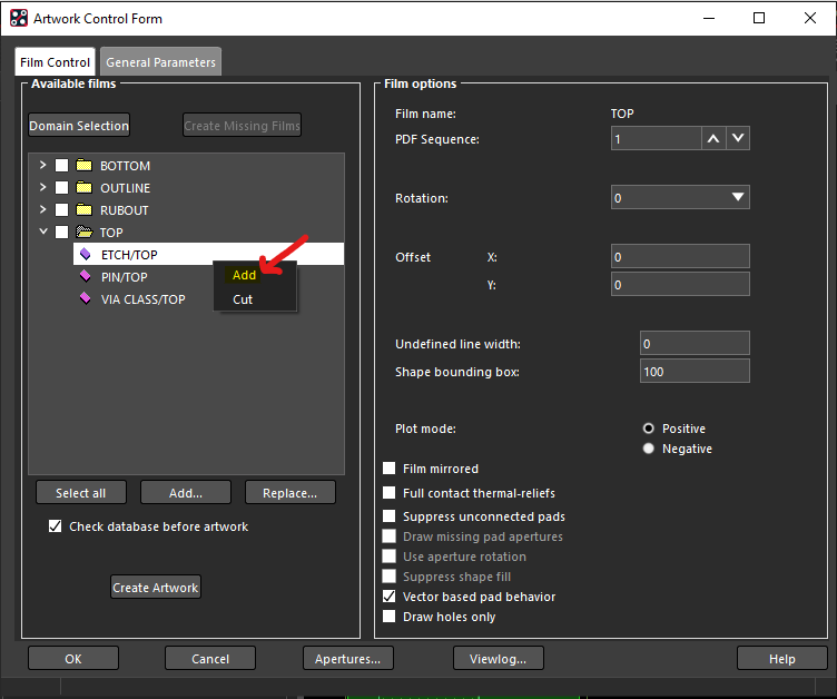
Figure 6: Add anti-etch layer

8. Then, expand the anti-etch subclass folder and select the box next to the layer you are adding it to (see Figure 7). Repeat this process for each layer that you have an anti-etch on.
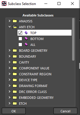
Figure 7: Adding the anti-etch layer to the top

9. Click the "Select all" button to output all of the layers

10. Click "Create Artwork" to export the Gerber files

11. Click "OK" to return to the layout

How do I export solder mask files from Cadence?

See the Exporting Solder Mask Layers from Cadence PCB Editor tutorial

How do I export drill files from Cadence?

  1. Open your PCB layout in Allegro PCB Designer
  2. Choose "Manufacture > NC > NC Drill..." The NC Drill window (see Figure 6) appears.

    Figure 6: NC Drill window

  3. Click "NC Parameters..." The NC Parameters window (see Figure 7) appears.

    Figure 7: NC Parameters window
  4. Select "Enhanced Excellon format" and click "Close"
  5. Name the drill file and save it in the same directory as your project
  6. Select "Auto tool select" and "Repeat codes"
  7. Click "Drill" to export the drill file
  8. Click "Close" to return to the layout

Thursday, September 17, 2015

Software design

What is a finite state machine?

A finite state machine (FSM) is a way of modeling a system such that there are a limited number of finite "states" that a system can be in, and that it can only be in one of those states at a time. Events (e.g., pushing a button) cause the system to change from one state to the next. Unexpected events do not cause the system to change states, which is useful for ignoring spurious inputs. Rather than coding for every possible input, you can instead code only for inputs that matter at the given time. The following resources provide a solid conceptual framing and implementation examples:

What is Unified Modeling Language™ (UML®)?

UML is an industry-standard specification for representing software designs. It is equivalent to schematics for hardware designs. More information on UML can be found at uml.org. Official documentation on UML is available at:
Common UML diagrams that you may use include:

What software do I use to create a UML diagram?

  • ArgoUML is an excellent free open-source software engineering tool that supports the creation of a wide variety of UML diagrams. It runs on Windows, Mac OS X, and Linux.
  • StarUML is another excellent freely-available program that supports the creation of a wide variety of UML diagrams. it runs on Windows, Mac OS X, and Linux.
  • Draw.Io - Recommended. Add-on to google drive documents, free - http://draw.io
  • LucidChart - cloud-based collaborative diagramming app ASU has a site license if you use your ASU google account.  Or get an Education Account.  Add as a addin via google drive.

What is pseudocode?

Pseudocode is a near-English representation of a program that allows you to represent the functionality of a program without worrying about the syntax. It is useful when planning how software will work. Pseudocode can be created in any text editor or word processing program. An example of pseudocode for the game Monopoly is available here.

Many links above suggested by Cecilia La Place

Sunday, September 13, 2015

What is a Gantt Chart?

A Gantt Chart is a common project management tool that helps teams understand the phases of a project, deadlines, critical paths, and interdependencies between tasks. It is important to gain experience predicting how long tasks take in order to calibrate your time management.

What software can I use to make a Gantt Chart?

Gantt Charts can be made with a variety of software programs. Here are several free options:
  • Microsoft Project - Available on MyApps (via Microsoft Imagine). This is the industry-standard project management tool (Windows)
  • ProjectLibre is an open-source alternative to Microsoft Project (Windows, Mac OS X, Linux)
  • RationalPlan Project Viewer is a Microsoft Project file viewer (Windows, Mac OS X, Linux)
  • Gantt charts can also be made in Microsoft Excel, but will not meet the dependency requirements in Dr. Jordan's assignment requirements.
  • Gantter is a cloud-based collaborative Gantt chart tool
  • Microsoft Visio is a general purpose graphical chart generation program with a nice Gantt chart template.  It is available on myapps.asu.edu through Microsoft Imagine

Monday, September 7, 2015

Transferring a Cadence schematic to PCB Editor

Introduction

In order to create a PCB, you must first prepare the schematic and check for errors, export a netlist of the schematic, import the netlist into PCB editor, and design the PCB. A netlist is a file that describes interconnections among components in a circuit. This tutorial describes the process of transferring a schematic to PCB Editor. It is assumed that you have a completed schematic (see example, Figure 1) before trying to migrate to PCB Editor.

Figure 1: Example schematic ready for transfer to PCB Editor

Video Walkthrough


1. Create Custom Footprints

All schematic symbols need a footprint. If you created any custom schematic symbols, you likely need to create a custom footprint for each one. For most ICs, you can use the Package Designer application to make custom footprints. For all other components, you can make custom footprints manually.

2. Open Project and Set Root Design

a) In Windows, open your project in the Design Entry CIS program.

b) For complex designs (see example, Figure 2), you may have multiple folders with multiple schematic sheets in each folder in the project explorer. Right-click on the folder you want to prepare for transfer to PCB Editor and choose "Make Root". This will set Cadence to generate a netlist only for the schematics inside the root folder (which will have a / through the folder symbol). This feature can be useful when your team is working on multiple break-out boards simultaneously before integrating them into one full design.

Figure 2: Example folder hierarchy for complex schematic

3. Assign Footprints to Components

c) Open the schematic and select all components on the page by choosing "Edit > Select All". Right-click and choose "Edit Properties..." (see Figure 3) to batch-edit the footprint information. The batch component property editing window will appear (see Figure 4). Click the Parts tab to show the parts in the schematic. Click the "Pivot" button to see the part information vertically instead of horizontally.

Figure 3: "Edit Properties..." menu option

Figure 4: Batch component property editing window

d) Enter footprint names (built-in or custom) for each component. For more information on finding the names of built-in footprints, see the "Where can I find a list of PCB footprints built-in to Cadence?" section on the Cadence PCB Tutorials page. Repeat until all components have footprints.

4. Run Design Rules Check

f) In the project explorer window, left-click on your schematic (see Figure 7) and choose "PCB menu > Design Rules Check" (see Figure 8). (If the Design Rules Check option is dimmed, then you have selected the wrong icon in the project explorer window). Figure 8 shows the Design Rules Check window. Leave the default options selected and click OK to continue.

Figure 7: Schematic icon selected

Figure 8: Design Rules Check... menu

Figure 9: Design Rules Check window

g) From there, you will be prompted with the DRC main screen in Figure 9. Keep everything as it is on the main screen and be sure to checkmark all of the boxes in the "Rules Setup" and "Report Setup" (see Figures 10 and 11). Doing this will ensure the DRC will check for many possible errors on the schematic. Once you have checked all of the boxes, click "Run".

Figure 10: Design Rules Check > Rules Setup pane

Figure 11: Design Rules Check > Report Setup pane

h) After you press "Run", several alerts will appear. The first will be to notify you that once you proceed with the DRC, all actions already made cannot be undone (see Figure 12). Click "Yes". The second will ask to save all the changes made since the last save (see Figure 13). Click "OK".

Figure 12: Undo Warning alert

Figure 13: Save changes alert

i) In the command window, you will see a list of warnings or errors that the DRC has found. If the "DRCs" window is blank, you are ready to move on and create your PCB design. If not and an error is listed (see example, Figure 14), go back to your schematic and fix the errors. If you see warnings, read each one and consider making the recommended changes before continuing. DO NOT SKIP THIS STEP. Fix any errors identified by the Design Rules Check and repeat steps (f) - (i) until all errors are gone (or determined not to be real problems).

Figure 14: DRCs error listing

5. Create a Netlist

h) In the project explorer window, left-click on your schematic and choose "Tools > Create Netlist..." (see Figure 15). (If the Create Netlist option is dimmed, then you have selected the wrong icon in the project explorer window). Figure 16 shows the Create Netlist window. Set the checkboxes as shown below (file names and paths will be specific to your design) and click OK to generate a netlist as shown in Figure 16. The setlist will appear in the folder you save it to. You do not need to open the file after creating it.

Figure 15: Tools > Create Netlist... menu

Figure 16: Create Netlist dialog box

6. Create/Update a Printed Circuit Board (PCB)

i) In the Project Explorer window, left-click on your schematic and choose "PCB menu > New Layout". (If the New Layout option is dimmed, then you have selected the wrong icon in the Project Explorer window). Figure 17 shows the New Layout window. Select the folder path where you would like yo create your new PCB design next to the "Board" path and click OK (see Figure 18). To update a PCB design you have already made, select the path where your current board is saved for "Input Board File" as well as for "Board", and click OK (see Figure 19). Once you have clicked OK, the Allegro PCB Editor will automatically open. See the Cadence PCB Tutorials page for more information on creating a PCB.

Figure 17: PCB > New Layout menu

Figure 18: New Layout window configured to create a new PCB design

Figure 19: New Layout window configured to update an existing PCB design

Common Errors

Schematic Updated after PCB is Routed

It's not uncommon for an error to be discovered in the schematic after the PCB has already been routed. Rework of routing can be fixed as follows:
  1. Fix the errors in the schematic
  2. In the project explorer window, left-click on your schematic (see Figure 7) and choose "Tools > Create Netlist...". (If the Create Netlist option is dimmed, then you have selected the wrong icon in the project explorer window). Figure 9 shows the Create Netlist window. Set the checkboxes as shown above (file names and paths will be specific to your design), but this time set "Input Board File" to be your current routed PCB file and "Output Board File" to be a different name for the updated file.
  3. Click OK to generate a netlist and push the changes forward to PCB Editor.

Duplicate Reference Designators

Sometimes, making significant edits to a schematic can result in multiple components with the same reference designators (e.g., U1, U2, R1, R2). This can be fixed by renumbering all of the reference designators in a schematic.

  1. Open the project in Design Entry CIS and select the *.dsn file in the project explorer.
  2. Choose "Tools > Annotate", select "Reset part references to "?"", and click OK (see Figure 10). Your schematic will now have ? marks for all reference designator numbers (e.g., U?, J?).
  3. Choose "Tools > Annotate" again, select "Incremental reference update", and click OK (see Figure 10). This will replace all ? marks with numbers to create unique reference designators.


Figure 10: Annotate window

Additional Common Errors

  • You changed your "nets" name but missed a trace somewhere
  • You changed your "nets" name and connected two different nets together accidentally (e.g., Ground_Plane and Ground)
  • Cadence couldn't find your footprint, or no footprint was specified
  • Missing a *.psm file for the *.dra file, or vice-versa
  • Unconnected traces
  • You used multiple ground symbols and connected them together incorrectly
  • Forgetting to define your paths correctly for footprints to be findable
  • Defining the footprint names for all parts.


Based on a tutorial by Josh Carroll

Cadence simulation tutorials

This page lists tutorials for doing circuit simulations in Cadence.

Getting Started


Techniques


Examples


PCB design checklist

Before exporting your PCB design for fabrication, you must verify the design and fix any errors. Time invested verifying your design before manufacturing will make the assembly and testing process significantly easier.

What are best practices for the design of PCBs?

General

  • All components have footprints
  • Bypass/decoupling capacitors for voltage regulators are placed as physically close as possible to the regulators
  • Bypass/decoupling capacitors for ICs are placed as physically close as possible to each IC's power and ground pins (see example of good layout, Figure 1)
  • Power and ground traces are at least 40 mil wide and were sized using a trace width calculator
  • Board space is allocated for mechanical constraints (e.g., PCB mounting holes, heat sinks, connectors)
  • The top and bottom copper layers are labeled in text "top", "bottom", and "group name"

Figure 1: Example of good bypass capacitor placement

Vias

  • Minimize the number of vias in your design. Vias reduce the reliability of your system.
  • No vias under components (particularly ICs)

Additional Considerations

  • Consider how your components will be mounted when routing traces. For example, if you have a through-hole connector on the top of your board, it's better to route the traces for it on the bottom layer.
  • Make the board outline in copper
  • Make sure that the size of your board will fit inside your product enclosure
  • Do NOT use the autorouter. Use manual routing to simplify the board design. Simple design = easier debugging.
  • When using surface mount components, size 0805 resistors and capacitors (or larger) are easier to work with
  • Through-hole connectors are mechanically stronger than surface-mount connectors
  • Avoid right angles (90 degrees) in traces. Instead, "curve" the trace with a 45 degree angle around a corner
  • Fill some extra space on your board with several 0.1" spaced test points to allow for easier modifications
  • If your system uses in-system programming (ISP), place the ISP connector as physically close to the microcontroller as possible


What is a printed circuit board?

A printed circuit board (PCB) is a board made of both conducive and non-conductive materials onto which components can be soldered to create a circuit. The circuit connections are made via copper traces on the board. An example PCB is shown in Figure 1.

Figure 1: Printed circuit board


Anatomy of a PCB

A PCB is made up of layers. Each layer represents a part of the manufacturing process (e.g., top and bottom copper layers, soldermask layer, silkscreen layer).

On the copper routing layers, components are soldered to copper footprints. A footprint is the physical layout on a PCB to which a component is soldered.

Each footprint has individual pads to which parts of the component (e.g., pins) are soldered.

How are PCBs manufactured?

In an industrial setting, PCBs are most commonly sent out to manufacturing houses that etch and return PCBs quickly but at very high cost. The following sites describe the PCB manufacturing process:
We are fortunate to have in-house PCB fabrication capabilities. See the What are our PCB fabrication capabilities? page for more information.

How do we manufacture PCBs at ASU?

See the ASU PCB Fabrication Process blog entry.

Sunday, September 6, 2015

Creating a custom PCB footprint manually in Cadence

Introduction

PCB footprint is the physical layout on a PCB to which a component is soldered. Usually, you must create a custom PCB footprint for each custom schematic symbol that you create. Footprints can be made for many standard components (e.g., basic ICs) using the Package Symbol Wizard (see the Creating a PCB footprint using Package Designer in Cadence page), but more complex components (like switching power supply ICs with thermal reliefs) must be created by hand. This tutorial details the manual creation of a custom footprint.

The example custom PCB footprint created in this tutorial will be a TI LM2676 SIMPLE SWITCHER® 8V to 40V, 3A Low Component Count Step-Down Regulator (see Figure 1).

Figure 1: LM2676 Switching Power Supply IC

1. Search the Datasheet for the Footprint Specifications

In order to build a custom footprint, you first need to find the footprint (sometimes called "land pattern" specifications in the datasheet for the component. Figures 2 and 3 show the land pattern and physical dimensions of the IC package from page 34 of the LM2676 datasheet.

Figure 2: Land pattern from the LM2676 datasheet. Dimensions are in mils, with brackets in mm.

Figure 3: Physical package dimensions from the LM2676 datasheet. Dimensions are in mils, with brackets in mm.

By interpreting Figures 2 and 3, the following key dimensions were determined:
  • Package geometry (overall)
    • Length = 565 mils
    • Width = 410 mils
  • Mechanical/Thermal Un-Plated Pad (underneath the body of the chip)
    • Length = 410 mils
    • Width = 425 mils
  • Pad - Pins
    • 7 total pins
    • Pad length = 36 mils
    • Pad width = 85 mils
    • Pad spacing = 50 mils (center of one pad to center of the next pad)

2. Create Custom Padstack(s)

For each different type of pin/pad, you need to create a custom padstack. For more information, see the Creating a custom padstack in Cadence page. For this example, you will need to create two custom padstacks using the dimensions above: one for the mechanical pad and one for the pin pads (which are all the same, so one padstack can be used).

3. Create a New Footprint

a) In Windows, open the PCB Editor application. (You can also use the Package Designer application).

b) Choose "File > New...". The New Drawing window shown in Figure 4 will appear.

Figure 4: New Drawing window

c) Name your drawing, select "Package symbol" and click OK. A blank package workspace will appear.

d) Since the component footprint is a rectangle (common), choose the "Shape Add Rect" tool (see Figure 5).

Figure 5: Toolbar

e) Move the cursor over the "Options" tab (see Figure 6) and enter the package geometry information from the datasheet. Then, place the rectangle on the blank workspace.

Figure 6: Options tab

f) Choose "Layout > Pins" to switch to pin mode. Move the cursor over the "Options" tab (see Figure 7). The options available in the tab are described below.

Figure 7: Layout > Pins - Options tab

The Connect and Mechanical options allow a choice between an electrical pin (Connect) and a mechanical or thermal relief (described in step i below).

The Padstack box and the "..." button allow entry of the path to the padstack file. These can be the same or different for each pin, depending on the land pattern in the component datasheet.

The Copy mode option allows selection of the coordinate system for your pins. Rectangular (default) is most common.

The X and Y options allow entry of the quantity, spacing (in mils), and order of pins being placed at once. Note that multiple pins placed this way will all use the same padstack (which in most cases is fine).

The Rotation option dictates which way the padstack will be rotated. This is particularly relevant when pins are wrapped around multiple sides of an IC (e.g., for a microcontroller).

The Pin # and Inc options allow entry of the starting pin number for the first pin and the number by which to increment pin numbers when multiple pins are placed simultaneously. Make sure that these pin numbers align with the pin numbers in the custom schematic symbol that you created.

The Text block and Text name options allow association of a name with the part.

The Offset X and Y options allow correction of spacing errors. If you have created your footprint correctly up to this point, you should not need this option.

g) Click on the "..." button next to Padstack. The "Select a padstack:" window will appear (see Figure 8). Make sure that both "Database" and "Library" are checked, and select the custom padstack that you created for the electrical pad. In this example, the custom padstack is called "Smd_85W36h", meaning that it is a surface mount part that is 85 mil wide and 36 mil high. Click OK.

Figure 8: Select a padstack window for electrical pad

h) Configure the rest of the Options window as shown in Figure 9 and click to place the first pin in the correct position inside the rectangle. The result (top view) should look like Figure 10.

Figure 9: Options for adding 7 custom pads

Figure 10: Pins added to footprint

This is a good time to double-check the data sheet connection diagrams to make sure the pin numbering is correct. Figure 11 shows the connection diagram for the IC package from page 2 of the LM2676 datasheet.

Figure 11: Connection diagram from LM2676 datasheet

Careful examination shows that our new symbol has pin 1 at the top of the footprint, whereas the datasheet indicates that pin 1 should be at the bottom of the footprint. This is a critical detail (and common mistake) that must be fixed in order for the board to work properly.

There are two ways to fix this problem.

OPTION 1: Delete and replace. Right-click in the workspace and choose "Done". Then, right-click on each pin and choose "Delete". Finally, re-place the pins using the corrected options shown in Figure 12.

Figure 12: Corrected options for adding 7 pads

OPTION 2: Manually Edit Text. Click the "Text Edit" tool in the toolbar (the bottom icon in Figure 13). Edit the number on each pin to correct it.

Figure 13: Toolbar with Text Edit tool (bottom)

The corrected footprint is shown in Figure 16.

i) Next, add the mechanical pad. Choose "Layout > Pins" to switch to pin mode. Move the cursor over the "Options" tab and click on the "..." button next to Padstack. Select the custom padstack that you created for the mechanical pad. In this example, the custom padstack is called "Lm2676_Mech" (see Figure 14). Click OK and place the pad in the correct position inside of the rectangle.

Figure 14: Select a padstack window for mechanical pad

j) Finally, you need to add a reference designator (RefDes) for the part number (in this example, LM2676) to the diagram. Click the Label Refdes tool (R1 button, second from the right in Figure 15) and add the part number above the footprint.

Figure 15: Label Refdes tool (second from right)


k) Finally, choose "File > Save As..." and save the footprint to your project folder. Do not use spaces in file names. Note that the Package Wizard creates two files: a DRA file (drawing of the package) and a PSM file (package symbol, footprint). The finished PCB footprint is shown in Figure 16.

Figure 16: Finished PCB footprint


Additional Resources


Based on a tutorial by Josh Carroll

Creating a custom padstack in Cadence

Introduction

A padstack is a design for the exposed copper surface area for each hole or pad on the board where the component is mounted and soldered (see example, Figure 1). You may need to create a custom padstack when creating custom parts to ensure that the pad and hole are big enough to be reliable. This tutorial describes the manual creation of custom padstacks using the Pad Designer application.

Figure 1: Padstack examples for through-hole and surface mount devies
The example below is for a simple round pad.  You should look up the dimensions for your own parts.

1. Search the Datasheet for the Footprint Specifications

In order to build a custom padstack, you first need to find the footprint (sometimes called "land pattern" specifications in the datasheet for the component. 

2. Create a Custom Electrical Padstack

1.    Open the new Padstack editor in Cadence:
2.    Select Thru-pin and circle on the start tab
3.    Enter the drill diameter
4.    Define the symbol that will be used to represent the drill hole:
5.    Define the Top and bottom layer inner, outer, and thermal geometry.  Since Peralta uses two-layer boards, geometry other than begin and end layers will be ignored.


The layers tab provides options for editing individual layers or the entire PCB. You can click on layers and make changes via the Regular Pad, Thermal Relief, and Anti Pad boxes described below.

The default layers for a padstack are:
  • BEGIN LAYER - top copper layer of the PCB
  • DEFAULT INTERNAL - inner layers of the PCB (our PCB mill is limited to 2 layers)
  • END LAYER - bottom copper layer of the PCB
  • SOLDERMASK_TOP - top colored soldermask layer of the PCB
  • SOLDERMASK_BOTTOM - bottom colored soldermask layer of the PCB
  • PASTEMASK_TOP - top solder paste layer of the PCB (uncommon in class)
  • PASTEMASK_BOTTOM - bottom solder paste layer of the PCB (uncommon in class)
  • FILMMASK_TOP - top conformal coating layer of the PCB (uncommon in class)
  • FILMMASK_BOTTOM - bottom conformal coating layer of the PCB (uncommon in class)
6.    Define the soldermask geometry for the top and bottom layers
7.    Look through the summary page to ensure everything was entered correctly:
8.    Save to the custom symbols folder you created and included in your padpath.


Additional Resources