Introduction
A
PCB footprint is the physical layout on a PCB to which a component is soldered. Usually, you must create a custom PCB footprint for each custom schematic symbol that you create. This tutorial details the easiest way to make custom footprints using the Package Symbol (Wizard).
1. Search the Datasheet for the Footprint Specifications
In order to build a custom footprint, you first need to find the footprint specifications in the datasheet for the component. However, sometimes a datasheet does not include a footprint. In this example, Cypress provides the
PCB design files for the PSoC® 4 CY8CKIT-049 4xxx Prototyping Kit, where you can get more useful information. Figure 2 shows the PCB layout provided by Cypress. Of note is that while it does show the dimensions of the PCB, it does not show the spacing or position of the pins in relation to the edges of the PCB. In this case, you will need a pair of calipers to measure the pin spacing and position of the pins in relation to the edge. Most standard header pins in embedded systems have a 100 mil (0.1") spacing between pins, but it is always good to double-check to avoid unnecessary PCB respins later. Additionally, this board can be "snapped" to separate the programmer (left) from the processor (right). This tutorial will assume that the programmer will be snapped off and only the processor module will be used.
 |
| Figure 2: Prototyping Kit PCB layout from Cypress |
Using this drawing and a pair of calipers to fill in missing information, the final dimensions were determined to be:
- Number of pins = 44 (22 per side)
- Lead pitch = 100 mils (0.1") - spacing from the center of one pin to the center of the next pin in a row
- Terminal row spacing = 750 mils (0.75") - spacing from the center of one row of pins to the center of the other row of pins
- Package width = 950 mils (0.95")
- Package length = 2300 mils (2.3")
2. Create a New Footprint
a) In Windows, open the PCB Editor application. (You can also use the Package Designer application).
b) Choose "File > New...". The New Drawing window shown in Figure 3 will appear.
 |
| Figure 3: New Drawing window |
c) Name your drawing (do not use spaces in drawing names), select "Package symbol (wizard)" and click OK. The Package Symbol Wizard window shown in Figure 4 will appear.
 |
| Figure 4: Package Symbol Wizard window |
d) Select the Package Type closest to the footprint that you are trying to make and click "Next >". The Package Symbol Wizard - Template window shown in Figure 5 will appear. For more information on package types, see the
IC Packages tutorial on Sparkfun. In this tutorial, the PSoC® footprint is closest to a Dual In-line Package (DIP), which is a common through-hole package.
 |
| Figure 5: Package Symbol Wizard - Template window |
e) In the Package Symbol Wizard - Template window, select "Default Cadence supplied template" and click "Load Template". Click "Next>" to continue to the "General Parameters" window (shown in Figure 6). The default template is generally good for most all footprints made using this wizard. Custom templates are required when the grid spacing is different, or if making very small parts (e.g., with QFN packages).
 |
| Figure 6: Package Symbol Wizard - General Parameters window |
f) The General Parameters window allows you to set the units that will be used to enter dimensions (typically "mils" for electronics applications) and the default prefix for the reference designator for this part. A reference designator is the unique ID labeling each part in a schematic (e.g., U1, U2, U3 for ICs). Click "Next >" to continue to the "DIP Parameters" window (see Figure 7).
 |
| Figure 7: Package Symbol Wizard - DIP Parameters window |
g) The DIP Parameters window allows you to enter the number of pins, spacing, width, and length of the footprint determined from the manufacturer (see step 1, above). Enter the appropriate information and click "Next >" to continue to the "Padstacks" window (See Figure 8).
 |
| Figure 8: Package Symbol Wizard - Padstacks window |
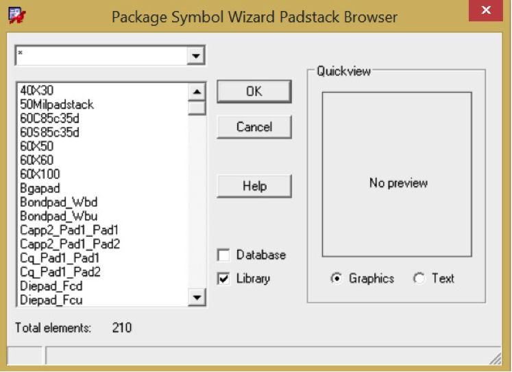
h) A padstack is a specification for the exposed copper surface area for each hole or pad on the board where the component is mounted and soldered. In our example, there are 44 pins that each use the same padstack. Click the "..." button next to "Default padstack to use for symbol pins" to display the padstack browser (see Figure 9).
 |
| Figure 9: Package Symbol Wizard Padstack Browser |
i) In the Padstack Browser window, choose a padstack that is appropriate for your component and click "Next >". The numbers are typically in mils (e.g., "Pad60cir42d" is a circular pad with diameter 60 mils and drill diameter of 42 mils). For through-hole components, it's usually better to have larger padstacks to allow for plenty of soldering area. For surface-mount components, the padstack should match the recommendations in the datasheet from the manufacturer. When in doubt, it's sometimes easier to make a custom padstack
(see the Creating a Custom Padstack in Cadence page).
 |
| Figure 10: Package Symbol Wizard - Symbol Compilation window |
j) The Symbol Compilation window appears (see Figure 10). Leave the default options selected and click "Next >" to show the Summary window (see Figure 11).
 |
| Figure 11: Package Symbol Wizard - Summary |
k) Finally, click "Finish" to complete the creation of the new symbol. A new window appears with the finished symbol (see Figure 12). Note that the Package Wizard creates two files: a DRA file (drawing of the package) and a PSM file (package symbol, footprint).
 |
| Figure 12: Finished PCB footprint |
Based on a tutorial by Josh Carroll


A great and interesting explanation of the PCB technology, thank you for that!
ReplyDelete