What is a ground plane?
A ground plane is a large area of copper in a printed circuit board design that is connected to ground on the power supply.What are advantages of having a ground plane in your PCB layout?
- Simpler circuit layout. All components with ground connections will automatically connect to the ground plane, rather than separate traces. Since most of your components will need to be connected to ground, this is a significant advantage.
- Larger current capacity. Ground planes are typically larger in area than typical PCB traces, meaning they can conduct larger return currents. This means that the ground potential across different parts of your circuit will be more similar and stable.
- Less electrical noise. When a digital component changes states (high -> low or low -> high), it creates electrical noise that travels throughout the circuit. Since ground planes have very low impedance, they "absorb" the electrical switching noise more effectively.
- Separate analog and digital grounds. For some (e.g., audio) circuits, it is necessary to have separate analog and digital grounds. With ground planes, you can make one layer of the board an analog ground plane and the other layer a digital ground plane, and connect them at a single point to minimize the effects of digital switching noise on the analog circuitry.
What are disadvantages of having a ground plane in your PCB layout?
- All traces and continuity must be carefully checked with a digital multimeter (DMM) before applying power to the board for the first time. (This is required even if you do not use a ground plane, but is even more important if you do.)
- When soldering and testing PCBs, ground planes make it extremely easy to accidentally short traces to ground. If the PCB manufacturing process leaves any extra copper behind (e.g., from milling), a power or signal trace may be connected directly to ground and short out components or power supplies when powering up the board.
- A DMM or oscilloscope probe can short a trace or component if the probe touches the powered trace and the ground plane simultaneously. Applying solder mask to the PCB will reduce (but not eliminate) this possibility.
- Sometimes, "ground islands" are created where a part of the ground plane is isolated from the rest of the circuit. A fix for this problem is described later in this tutorial.
How do you create a ground plane in an existing PCB layout?
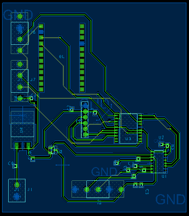
1. Start with a PCB layout that has a board layout, all components placed, and all traces routed except the ground traces (see example with ground traces in blue, Figure 1). As you can see, routing all of the ground traces in the example below would add a lot of complexity, so adding a ground plane is a good design option. |
| Figure 1: Example PCB layout with un-routed ground traces in blue |
2. In the toolbar, click on the Add Rectangle tool (see Figure 2) and select the "Options" tab on the right side of the screen (see Figure 3). Do not draw a rectangle yet.

Figure 2: Add rectangle tool
| Figure 3: Options tab for the Add Rectangle tool |

3. In the Options tab, click on the "..." button (see Figure 4) near "Assign net name" and choose your ground net (see Figure 5). Click OK to close the "Select a net" dialog box.
| Figure 4: "..." button to assign ground net name |

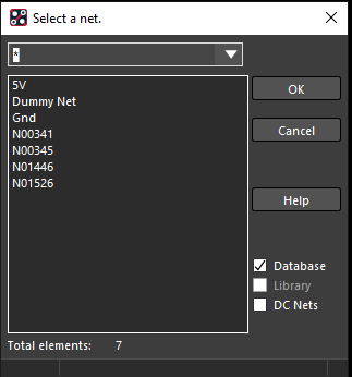
| Figure 5: "Select a net" dialog box |
4. Draw a rectangle around all of the placed components. If the above steps were completed correctly, the blue rats nest connections should disappear and ground pins electrically connected to the ground plane (see example, Figure 6).
 |
| Figure 6: Ground rectangle placed |
Figures 7 and 8 below show closeups "before ground plane" and "after ground plane" connections.
 |
| Figure 7: Closeup of board design before ground plane |
 |
| Figure 8: Closeup of board design after ground plane |
As you can see in Figure 8 above, the connections between the ground pins and the ground plane are very small (5 mils), making them a potential point of unreliability or failure in the design. Connections to power and ground should be a minimum of 20 mils, or larger if using higher currents (use a trace width calculator to determine the minimum size).
5. To increase the size of the connections between pins and the ground plane, choose Shape > Global Dynamic Params... (see Figure 9).
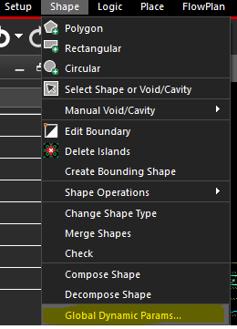
| Figure 9: Global Dynamic Parameters menu option |
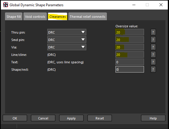
6. Select the "Clearances" tab (see Figure 10) and update the oversize values to a larger number (20 mils or greater) to make the design easier to manufacture and test.
| Figure 10: Clearances tab with updated oversize clearance values |
7. Select the "Thermal relief connects" tab (see Figure 11) and update the thermal width to a larger number (20 mils, or greater for higher currents). Click "OK" to apply the changes.
| Figure 11: Thermal relief connects tab with updated thermal width |

Figures 12 and 13 below show closeups before and after the changes to the global dynamic parameters. Note that changes are applied to the entire design, not just a single pad.
 |
| Figure 12: Example pad before global dynamic parameters adjustments |
 |
| Figure 13: Example pad after global dynamic parameters adjustments |
How do I find and eliminate ground islands?
A "ground island" is a section of a ground plane that is isolated from the rest of the circuit. Ground islands can often be discovered through careful examination of a design with a ground plane, noticing where a rats nest wire still exists (see example, Figure 14). |
| Figure 14: Example "ground island" |
A ground island can be fixed by adding a via between the ground island and the remainder of the ground plane (see example, Figure 15).
 |
| Figure 15: Repaired ground island |
 |
| Figure 16: Completed PCB design with ground plane |
What is a void, rubout, or anti-etch and when do I use one?
A void, rubout, or anti-etch is a place where the copper is fully removed from the PCB. A common use of rubouts is underneath Bluetooth or Wifi antennas (e.g., from a Photon or Argon) as having a ground plane underneath an antenna will effectively shield RF waves from reaching the antenna. At best this will mean reduced range for a wireless device, and at worst it will mean that the device will not connect wirelessly.
How do I create a rubout in Cadence?
1. First, make sure you have placed all of the components on your PCB (and ideally have not started routing traces yet, though this can still be done even if you have routed traces).
2. Choose Shape > Manual Void/Cavity and choose a shape of your liking (see Figure 17).
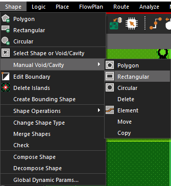
Figure 17: Anti-etch selection
3. Draw an anti-etch on the appropriate layer(s) in appropriate place(s) (e.g., underneath an antenna). If there are existing races or vias in the area of the anti-etch, you will need to move them. If you have ground (or power) planes on multiple layers, you should place an anti-etch on each of the copper layers (e.g., TOP and BOTTOM). See example in Figure 18.
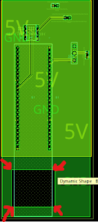
Figure 18: Anti-etch example under a PSoC® 5 footprint
4. To delete an anti-etch, you need to use the special delete tool in the Manual Void/Cavity menu (see Figure 19).

Figure 19: Delete tool for manual void/cavity
5. When generating your final Gerber files, you will need to add these anti-etches to the layers in the Artwork Control Form in order for them to be manufactured (see How do I export Gerber files from Cadence?).
Additional Resources
- Tutorial on Split Planes from parsysEDA
Based on a tutorial by Cody Van Cleve and updated by Jacob Lara in 2020.


Thanks for providing recent updates regarding the concern, I look forward to read more. d499r
ReplyDelete