Introduction
This tutorial will walk through the creation of a custom surface-mount device (SMD) footprint manually. A MCH3382 Power MOSFET from ON Semiconductor will be used as an example.
How do you create a custom SMD pad manually in Cadence?
1. First, find the soldering footprint (sometimes named slightly differently, depending on manufacturer) in the component datasheet (see Figure 1).
 |
| Figure 1: Recommended soldering footprint for MCH3382 Power MOSFET |
2. In Windows, open Pad Editor in the Cadence folder in the Start Menu. The Pad Editor window will appear (see Figure 2). The pad editor will allow you to create a padstack for the three individual pads in the footprint. Select "SMD Pin" under "Select padstack usage:" and select "Rectangle" under "Select the default pad geometry".
 |
| Figure 2: Pad Editor main window |
3. In the "Units" section of the Pad Editor window (located in the bottom left corner), change the units to match the units in the component datasheet (see Figure 2). For the MCH3382, the footprint is in millimeters (mm).
4. Click the Design Layers tab and select the BEGIN LAYER (see Figure 3). Choose a Geometry of Rectangle and enter the width and height (found in the component data sheet) of a single pad.
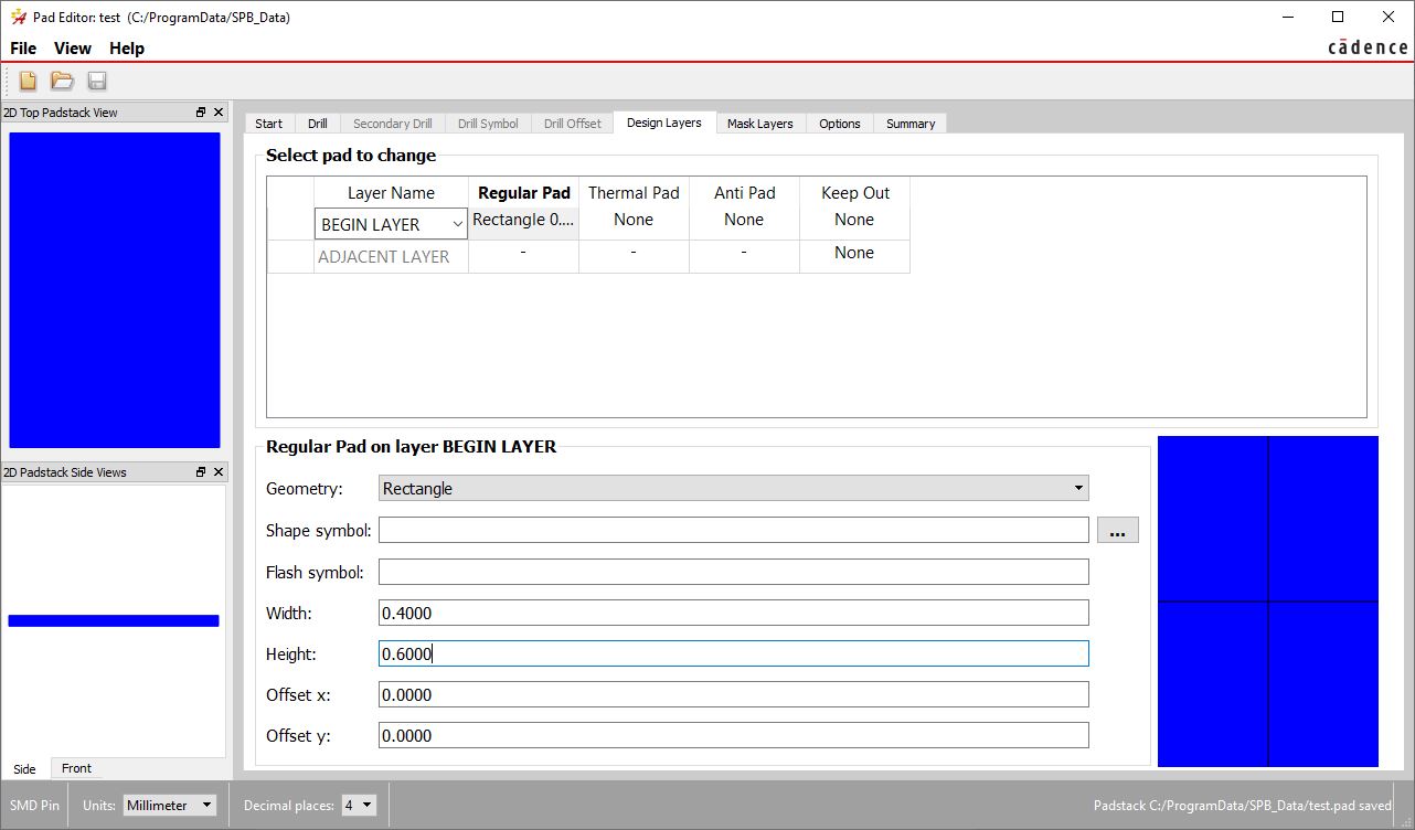 |
| Figure 3: Layers tab with BEGIN LAYER and Rectangle Pad selected |
5. Save the padstack in the same location as your custom symbols. The following folder is the default:
C:\Program Files\Cadence\SPB_17.2\share\pcb\pcb_lib\symbols
6. Repeat steps 1 - 5 for any additional different pads in your component. You do not need to recreate the same pad if it is used multiple times in a single footprint.
How do you create a custom SMD footprint manually in Cadence?
1. Open PCB Editor and create a "New Drawing". Name the drawing after the package name, and set the "Drawing Type" to Package symbol (see Figure 4). Click OK.
 |
| Figure 4: New Drawing dialog box |
2. Select the Color Picker to adjust the footprint colors to contrast against the black background (see Figure 5).
| Figure 5: Color Dialog with all subclasses set to white for better contrast |
3. In the Color selection, select white and double-click on the white box beside the All subclass to set all of the subclasses to white (see Figure 5). Click OK.
4. Choose Setup > Grids... to adjust the grid layout and spacing. In the Define Grid dialog, check the "Grids On" checkbox, enter 0.1 for the Spacing in both the x and y dimensions, and click OK (see Figure 6).
 |
| Figure 6: Define Grid dialog |
5. Zoom in and find the white origin mark
6. Choose Layout > Pins and click on the "Options" tab on the right side of the screen (see Figure 7).
 |
| Figure 7: Options tab for the Pin layout tool |
7. Click the "..." button next to "Padstack" and select the padstack that you made in the first part of this tutorial.
8. Determine an origin for your footprint based on the measurements in the datasheet. For the MCH3382, the origin will be where the vertical and horizontal measurement lines intersect in the bottom center of the footprint (see Figure 8).
|
| Figure 8: Recommended soldering footprint for MCH3382 Power MOSFET |
9. In the Command window at the bottom of the screen, type x -65 0 to place the first pad to the left of the origin. Type x 65 0 to place the second pad to the right of the origin, and x 0 210 to place the third pad above.
10. Next, add a box around the footprint so that it is clear the pads are related when laying out the printed circuit board. Select the Rectangle tool in the toolbar, and click the Options tab on the right side of the screen. Set the "Active Class and Subclass" to Package Geometry and Assembly_Top, respectively.
11. In the Command window at the bottom of the screen, type x -80 0 and press return to place the left corner of the box. Then, type x 80 210 to place the top right corner of the box. Right-click and select "Done". The footprint should now look like Figure 9.
 |
| Figure 9: Footprint after adding pads |
12. Next, we need to add a reference designator that will be visible in the PCB layout. Choose Layout > Labels > RefDes. Select the center of the component and type "U?". Right-click and select "Done". The footprint should now look like Figure 10.
 |
| Figure 10: Footprint after adding reference designator |
13. Save and close PCB Editor. You have successfully made a custom SMD footprint!
Based on a tutorial by Aaron Dolgin, updated by Sheena Benson (2/2020)


No comments:
Post a Comment