Step 1. Create a Cadence Folder Hierarchy
In order for both you and Cadence to find your files easily, download the custom Cadence folder hierarchy ZIP file to your computer and decompress it on the desktop. The resultant folder hierarchy is as follows:
- Desktop\Cadence\Backups - All backups saved by Design Entry CIS and PCB Editor will be saved here.
- Desktop\Cadence\Projects - All project files that you generate should be saved here. Inside this folder, create a separate folder for each project or schematic so that the files do not get mixed up when you create a new project.
- Desktop\Cadence\step - All .step files that you download or make to use with the PCB Editor 3-D View function should be stored in this folder. Downloadable .step files can be found at 3D Content Central.
- Desktop\Cadence\symbols - All .pad, .bsm, .psm, and .dra files that you download or make should be stored in this folder. These files contain component footprints and mechanical pins that are used by Cadence. This folder also contains a special ASU via padstack (asuvia.pad) that improves manufacturability on the LPKF PCB mill in PRLTA 109.
Step 2. Configure Capture CIS
CAPTURE.INI is the primary file in which Cadence stores all of the program settings for schematic editing in Capture CIS. We have created a custom CAPTURE.INI file for the ASU Polytechnic School engineering programs. Follow the instructions below to install and modify the custom CAPTURE.INI file:
1. Open the Capture CIS application, which you will use to design schematics. When the "Cadence Product Choices" window (see Figure 4) appears, select Allegro PCB Design CIS L and click the checkbox next to Use as default. Click OK to continue.
1. Open the Capture CIS application, which you will use to design schematics. When the "Cadence Product Choices" window (see Figure 4) appears, select Allegro PCB Design CIS L and click the checkbox next to Use as default. Click OK to continue.
 |
| Figure 1: Cadence Product Choices window |
2. Quit the "Capture CIS 17.4" application.
3. Download the ASU Polytechnic School custom Capture.INI file to your computer. This custom file configures Cadence as follows:
- Tells Capture CIS to look for PCB footprints in both C:\Program Files\Cadence\SPB_17.4\share\pcb\pcb_lib\symbols and in C:\Users\YOURWINDOWSLOGIN\Desktop\Cadence\symbols.
- Turns on autosave to save your Capture CIS design every 10 minutes.
- Turns on auto backup to back up your Capture CIS design every 10 minutes to C:\Users\YOURWINDOWSLOGIN\Desktop\Cadence\Backups.
- Adds two custom help links to the Capture CIS > Help > Web Resources menu
4. Edit the custom CAPTURE.INI file to replace the two instances of the text YOURWINDOWSLOGIN with your Windows login (where your home directory is located) on your computer. Examples:
DIR1=C:\Users\YOURWINDOWSLOGIN\Desktop\Cadence\symbols
to
DIR1=C:\Users\ssjorda1\Desktop\Cadence\symbols
Backup Direcory Path=C:\Users\YOURWINDOWSLOGIN\Desktop\Cadence\Backups
to
Backup Direcory Path=C:\Users\ssjorda1\Desktop\Cadence\Backups
Figure 2 below shows the original custom CAPTURE.INI file, and Figure 3 below shows an edited example.
5. Copy your edited custom CAPTURE.INI file to replace the default CAPTURE.INI file at one of the following paths:
C:\ProgramData\SPB_Data\cdssetup\OrCAD_Capture\17.4.0\Capture.ini
%HOME%\cdssetup\OrCAD_Capture\17.4.0\Capture.ini
where %HOME% is the location you set as your home directory (typcically "c:/users/YOURUSERNAME")
or
C:\Cadence\SPB_Data-Silent\cdssetup\OrCAD_Capture\17.4.0\Capture.ini
or if you have defined your home directory differently according to the installation instructions, use
%HOME%\cdssetup\OrCAD_Capture\17.4.0\Capture.ini
where %HOME% is the location you set as your home directory (typcically "c:/users/YOURUSERNAME")
 |
| Figure 2: Original custom CAPTURE.INI template |
 |
| Figure 3: Example edited custom CAPTURE.INI template |
Step 3. Configure PCB Editor
1. Open the PCB Editor application, which you will use to create PCB designs. When the "17.4 Allegro PCB Designer Product Choices" window (see Figure 4) appears, select Allegro PCB Designer and click the checkbox next to Use as default. Click OK to continue. |
| Allegro PCB Designer Product Choices window |
2. Choose Setup > User Preferences... (see Figure 5).
 |
| Figure 5: Setup > User Preferences... menu option |
3. Turn on autosave in PCB Editor to automatically back up your design in case of a system crash by selecting the File_management > Autosave category and changing the settings to match the configuration shown in Figure 6 below. Note: By selecting the Favorite check box, PCB Editor will make it easier to access these settings in the future by saving them in the My_favorites folder at the top of the Categories list.
 |
| Figure 6: User Preferences Editor Autosave category configuration |
4. Configure the search paths in PCB Editor by selecting the Paths > Library category and selecting the Favorite checkboxes next to padpath, psmpath, and steppath (see Figure 7).
 |
| Figure 7: User Preferences Editor Paths > Library window |
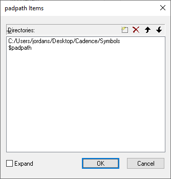
5. Click the ... next to padpath and add the path to the symbols folder in the Cadence folder on your desktop (C:/Users/YOURWINDOWSLOGIN/Desktop/Cadence/symbols) (see Figure 8). Click the up button to give your library priority over the default location(s). Click OK to save changes.
 |
| Figure 8: Adding to the padpath example |
6. Click the ... next to psmpath and add the path to the symbols folder in the Cadence folder on your desktop (C:/Users/YOURWINDOWSLOGIN/Desktop/Cadence/symbols) (see Figure 9). Click the up button to give your library priority over the default location(s). Click OK to save changes.
 |
| Figure 9: Adding to the psmpath example |
7. Click the ... next to steppath and add the path to the step folder in the Cadence folder on your desktop (C:/Users/YOURWINDOWSLOGIN/Desktop/Cadence/step) (see Figure 10). Click the up button to give your library priority over the default location(s). Click OK to save changes.
 |
| Figure 10: Adding to the steppath example |
Congratulations, you have configured Cadence!
Next: Get started creating a schematicCommon Issues
If you can't find your config.ini file, make sure you
Also, here is a video documenting an older version of this process:


No comments:
Post a Comment